


MOSFET


The metal–oxide–semiconductor field-effect transistor (MOSFET, MOS-FET, or MOS FET) is a transistor used for amplifying or switching electronic signals. The basic principle of this kind of transistor was first proposed by Julius Edgar Lilienfeld in 1925. In MOSFETs, a voltage on the oxide-insulated gate electrode can induce a conducting channel between the two other contacts called source and drain. The channel can be of n-type or p-type (see article on semiconductor devices), and is accordingly called an nMOSFET or a pMOSFET (also commonly nMOS, pMOS). It is by far the most common transistor in both digital and analog circuits, though the bipolar junction transistor was at one time much more common.
The 'metal' in the name is now often a misnomer because the previously metal gate material is now often a layer of polysilicon (polycrystalline silicon). Aluminium had been the gate material until the mid 1970s, when polysilicon became dominant, due to its capability to form self-aligned gates. Metallic gates are regaining popularity, since it is difficult to increase the speed of operation of transistors without metal gates.
IGFET is a related term meaning insulated-gate field-effect transistor, and is almost synonymous with MOSFET, though it can refer to FETs with a gate insulator that is not oxide. Another synonym is MISFET for metal–insulator–semiconductor FET.
Contents[hide]
|
[edit] Composition

Usually the semiconductor of choice is silicon, but some chip manufacturers, most notably IBM and Intel, recently started using a chemical compound of silicon and germanium (SiGe) in MOSFET channels. Unfortunately, many semiconductors with better electrical properties than silicon, such as gallium arsenide, do not form good semiconductor-to-insulator interfaces, thus are not suitable for MOSFETs. Research continues on creating insulators with acceptable electrical characteristics on other semiconductor material.
In order to overcome power consumption increase due to gate current leakage, high-κ dielectric replaces silicon dioxide for the gate insulator, while metal gates return by replacing polysilicon (see Intel announcement[1]).
The gate is separated from the channel by a thin insulating layer, traditionally of silicon dioxide and later of silicon oxynitride. Some companies have started to introduce a high-κ dielectric + metal gate combination in the 45 nanometer node.
When a voltage is applied between the gate and body terminals, the electric field generated penetrates through the oxide and creates an "inversion layer" or "channel" at the semiconductor-insulator interface. The inversion channel is of the same type, P-type or N-type, as the source and drain, thus it provides a channel through which current can pass. Varying the voltage between the gate and body modulates the conductivity of this layer and allows to control the current flow between drain and source.
[edit] Circuit symbols
A variety of symbols are used for the MOSFET. The basic design is generally a line for the channel with the source and drain leaving it at right angles and then bending back at right angles into the same direction as the channel. Sometimes three line segments are used for enhancement mode and a solid line for depletion mode. Another line is drawn parallel to the channel for the gate.
The bulk connection, if shown, is shown connected to the back of the channel with an arrow indicating PMOS or NMOS. Arrows always point from P to N, so an NMOS (N-channel in P-well or P-substrate) has the arrow pointing in (from the bulk to the channel). If the bulk is connected to the source (as is generally the case with discrete devices) it is sometimes angled to meet up with the source leaving the transistor. If the bulk is not shown (as is often the case in IC design as they are generally common bulk) an inversion symbol is sometimes used to indicate PMOS, alternatively an arrow on the source may be used in the same way as for bipolar transistors (out for nMOS, in for pMOS).
Comparison of enhancement-mode and depletion-mode MOSFET symbols, along with JFET symbols (drawn with source and drain ordered such that higher voltages appear higher on the page than lower voltages):
 |
 |
 |
 |
 |
P-channel |
 |
 |
 |
 |
 |
N-channel |
| JFET | MOSFET enh | MOSFET enh (no bulk) | MOSFET dep | ||
For the symbols in which the bulk, or body, terminal is shown, it is here shown internally connected to the source. This is a typical configuration, but by no means the only important configuration. In general, the MOSFET is a four-terminal device, and in integrated circuits many of the MOSFETs share a body connection, not necessarily connected to the source terminals of all the transistors.
[edit] MOSFET operation


[edit] Metal–oxide–semiconductor structure
A traditional metal–oxide–semiconductor (MOS) structure is obtained by growing a layer of silicon dioxide (SiO2) on top of a silicon substrate and depositing a layer of metal or polycrystalline silicon (the latter is commonly used). As the silicon dioxide is a dielectric material, its structure is equivalent to a planar capacitor, with one of the electrodes replaced by a semiconductor.
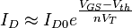
When a voltage is applied across a MOS structure, it modifies the distribution of charges in the semiconductor. If we consider a P-type semiconductor (with NA the density of acceptors, p the density of holes; p = NA in neutral bulk), a positive voltage, VGB, from gate to body (see figure) creates a depletion layer by forcing the positively charged holes away from the gate-insulator/semiconductor interface, leaving exposed a carrier-free region of immobile, negatively charged acceptor ions (see doping (semiconductor)). If VGB is high enough, a high concentration of negative charge carriers forms in an inversion layer located in a thin layer next to the interface between the semiconductor and the insulator. Unlike the MOSFET, where the inversion layer electrons are supplied rapidly from the source/drain electrodes, in the MOS capacitor they are produced much more slowly by thermal generation through carrier generation and recombination centers in the depletion region. Conventionally, the gate voltage at which the volume density of electrons in the inversion layer is the same as the volume density of holes in the body is called the threshold voltage.
This structure with p-type body is the basis of the N-type MOSFET, which requires the addition of an N-type source and drain regions.
[edit] MOSFET structure and channel formation


A metal–oxide–semiconductor field-effect transistor (MOSFET) is based on the modulation of charge concentration by a MOS capacitance between a body electrode and a gate electrode located above the body and insulated from all other device regions by a gate dielectric layer which in the case of a MOSFET is an oxide, such as silicon dioxide. If dielectrics other than an oxide such as silicon dioxide (often referred to as oxide) are employed the device may be referred to as a metal–insulator–semiconductor FET (MISFET). Compared to the MOS capacitor, the MOSFET includes two additional terminals (source and drain), each connected to individual highly doped regions that are separated by the body region. These regions can be either p or n type, but they must both be of the same type, and of opposite type to the body region. The source and drain (unlike the body) are highly doped as signified by a '+' sign after the type of doping.
If the MOSFET is an n-channel or nMOS FET, then the source and drain are 'n+' regions and the body is a 'p' region. As described above, with sufficient gate voltage, holes from the body are driven away from the gate, forming an inversion layer or n-channel at the interface between the p region and the oxide. This conducting channel extends between the source and the drain, and current is conducted through it when a voltage is applied between source and drain. Increasing the voltage on the gate leads to a higher electron density in the inversion layer and therefore increases the current flow between the source and drain.
For gate voltages below the threshold value, the channel is lightly populated, and only a very small subthreshold leakage current can flow between the source and the drain.
If the MOSFET is a p-channel or pMOS FET, then the source and drain are 'p+' regions and the body is a 'n' region. When a negative gate-source voltage (positive source-gate) is applied, it creates a p-channel at the surface of the n region, analogous to the n-channel case, but with opposite polarities of charges and voltages. When a voltage less negative than the threshold value (a negative voltage for p-channel) is applied between gate and source, the channel disappears and only a very small subthreshold current can flow between the source and the drain.
The source is so named because it is the source of the charge carriers (electrons for n-channel, holes for p-channel) that flow through the channel; similarly, the drain is where the charge carriers leave the channel.
The device may comprise a Silicon On Insulator (SOI) device in which a Buried OXide (BOX) is formed below a thin semiconductor layer. If the channel region between the gate dielectric and a Buried Oxide (BOX) region is very thin, the very thin channel region is referred to as an Ultra Thin Channel (UTC) region with the source and drain regions formed on either side thereof in and/or above the thin semiconductor layer. Alternatively, the device may comprise a SEMiconductor On Insulator (SEMOI) device in which semiconductors other than silicon are employed. Many alternative semiconductor materials may be employed.
When the source and drain regions are formed above the channel in whole or in part, they are referred to as Raised Source/Drain (RSD) regions.
[edit] Modes of operation
The operation of a MOSFET can be separated into three different modes, depending on the voltages at the terminals. In the following discussion, a simplified algebraic model is used that is accurate only for old technology. Modern MOSFET characteristics require computer models that have rather more complex behavior.
For an enhancement-mode, n-channel MOSFET, the three operational modes are:
- Cutoff, subthreshold, or weak-inversion mode
- When VGS < Vth:
- where Vth is the threshold voltage of the device.
- According to the basic threshold model, the transistor is turned off, and there is no conduction between drain and source. In reality, the Boltzmann distribution of electron energies allows some of the more energetic electrons at the source to enter the channel and flow to the drain, resulting in a subthreshold current that is an exponential function of gate–source voltage. While the current between drain and source should ideally be zero when the transistor is being used as a turned-off switch, there is a weak-inversion current, sometimes called subthreshold leakage.
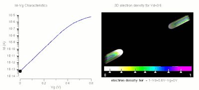
- In weak inversion the current varies exponentially with gate-to-source bias VGS as given approximately by:[3][4]
-
 ,
,
- where ID0 = current at VGS = Vth, the thermal voltage VT = kT / q and the slope factor n is given by
-
- n = 1 + CD / COX,
- with CD = capacitance of the depletion layer and COX = capacitance of the oxide layer. In a long-channel device, there is no drain voltage dependence of the current once VDS > > VT, but as channel length is reduced drain-induced barrier lowering introduces drain voltage dependence that depends in a complex way upon the device geometry (for example, the channel doping, the junction doping and so on). Frequently, threshold voltage Vth for this mode is defined as the gate voltage at which a selected value of current ID0 occurs, for example, ID0 = 1 μA, which may not be the same Vth-value used in the equations for the following modes.
- Some micropower analog circuits are designed to take advantage of subthreshold conduction.[5][6][7] By working in the weak-inversion region, the MOSFETs in these circuits deliver the highest possible transconductance-to-current ratio, namely: gm / ID = 1 / (nVT), almost that of a bipolar transistor.[8]
- The subthreshold I–V curve depends exponentially upon threshold voltage, introducing a strong dependence on any manufacturing variation that affects threshold voltage; for example: variations in oxide thickness, junction depth, or body doping that change the degree of drain-induced barrier lowering. The resulting sensitivity to fabricational variations complicates optimization for leakage and performance.[9][10]


- Triode mode or linear region (also known as the ohmic mode[11][12])
- When VGS > Vth and VDS < ( VGS – Vth )
- The transistor is turned on, and a channel has been created which allows current to flow between the drain and the source. The MOSFET operates like a resistor, controlled by the gate voltage relative to both the source and drain voltages. The current from drain to source is modeled as:
-

- where μn is the charge-carrier effective mobility, W is the gate width, L is the gate length and Cox is the gate oxide capacitance per unit area. The transition from the exponential subthreshold region to the triode region is not as sharp as the equations suggest.
- Saturation or active mode[13][14]
- When VGS > Vth and VDS > ( VGS – Vth )
- The switch is turned on, and a channel has been created, which allows current to flow between the drain and source. Since the drain voltage is higher than the gate voltage, the electrons spread out, and conduction is not through a narrow channel but through a broader, two- or three-dimensional current distribution extending away from the interface and deeper in the substrate. The onset of this region is also known as pinch-off to indicate the lack of channel region near the drain. The drain current is now weakly dependent upon drain voltage and controlled primarily by the gate–source voltage, and modeled approximately as:
-

- The additional factor involving λ, the channel-length modulation parameter, models current dependence on drain voltage due to the Early effect, or channel length modulation. According to this equation, a key design parameter, the MOSFET transconductance is:
 ,
,
- where the combination Vov = VGS – Vth is called the overdrive voltage,[15] and where VDSsat = VGS - Vth (which Sedra neglects) accounts for a small discontinuity in ID which would otherwise appear at the transition between the triode and saturation regions.
- Another key design parameter is the MOSFET output resistance rout given by:
 .
. - rout is the inverse of gDS where
 . VDS is the expression in saturation region.
- If λ is taken as zero, an infinite output resistance of the device results that leads to unrealistic circuit predictions, particularly in analog circuits.
- As the channel length becomes very short, these equations become quite inaccurate. New physical effects arise. For example, carrier transport in the active mode may become limited by velocity saturation. When velocity saturation dominates, the saturation drain current is more nearly linear than quadratic in VGS. At even shorter lengths, carriers transport with near zero scattering, known as quasi-ballistic transport. In addition, the output current is affected by drain-induced barrier lowering of the threshold voltage.
[edit] Body effect

The body effect describes the changes in the threshold voltage by the change in the source-bulk voltage, approximated by the following equation:
 ,
,
where VTN is the threshold voltage with substrate bias present, and VTO is the zero-VSB value of threshold voltage, γ is the body effect parameter, and 2φ is the surface potential parameter.
The body can be operated as a second gate, and is sometimes referred to as the "back gate"; the body effect is sometimes called the "back-gate effect".[16]
[edit] History
In 1959, Dawon Kahng and Martin M. (John) Atalla at Bell Labs invented the metal–oxide–semiconductor field-effect transistor (MOSFET).[17] Operationally and structurally different from the bipolar junction transistor,[18] the MOSFET was made by putting an insulating layer on the surface of the semiconductor and then placing a metallic gate electrode on that. It used crystalline silicon for the semiconductor and a thermally oxidized layer of silicon dioxide for the insulator. The silicon MOSFET did not generate localized electron traps at the interface between the silicon and its native oxide layer, and thus was inherently free from the trapping and scattering of carriers that had impeded the performance of earlier field-effect transistors. Following the (expensive) development of clean rooms to reduce contamination to levels never before thought necessary, and of photolithography[19] and the planar process to allow circuits to be made in very few steps, the Si–SiO2 system possessed such technical attractions as low cost of production (on a per circuit basis) and ease of integration. Largely because of these two factors, the MOSFET has become the most widely used type of transistor in integrated circuits.
[edit] CMOS circuits
The MOSFET is used in digital CMOS logic,[20] which uses p- and n-channel MOSFETs as building blocks. Overheating is a major concern in integrated circuits since ever more transistors are packed into ever smaller chips. CMOS logic reduces power consumption because no current flows (ideally), and thus no power is consumed, except when the inputs to logic gates are being switched. CMOS accomplishes this current reduction by complementing every nMOSFET with a pMOSFET and connecting both gates and both drains together. A high voltage on the gates will cause the nMOSFET to conduct and the pMOSFET not to conduct and a low voltage on the gates causes the reverse. During the switching time as the voltage goes from one state to another, both MOSFETs will conduct briefly. This arrangement greatly reduces power consumption and heat generation. Digital and analog CMOS applications are described below.
[edit] Digital
The growth of digital technologies like the microprocessor has provided the motivation to advance MOSFET technology faster than any other type of silicon-based transistor.[21] A big advantage of MOSFETs for digital switching is that the oxide layer between the gate and the channel prevents DC current from flowing through the gate, further reducing power consumption and giving a very large input impedance. The insulating oxide between the gate and channel effectively isolates a MOSFET in one logic stage from earlier and later stages, which allows a single MOSFET output to drive a considerable number of MOSFET inputs. Bipolar transistor-based logic (such as TTL) does not have such a high fanout capacity. This isolation also makes it easier for the designers to ignore to some extent loading effects between logic stages independently. That extent is defined by the operating frequency: as frequencies increase, the input impedance of the MOSFETs decreases.
[edit] Analog
The MOSFET's advantages in digital circuits do not translate into supremacy in all analog circuits. The two types of circuit draw upon different features of transistor behavior. Digital circuits switch, spending most of their time outside the switching region, while analog circuits depend on MOSFET behavior held precisely in the switching region of operation. The bipolar junction transistor (BJT) has traditionally been the analog designer's transistor of choice, due largely to its higher transconductance and its higher output impedance (drain-voltage independence) in the switching region.
Nevertheless, MOSFETs are widely used in many types of analog circuits because of certain advantages. The characteristics and performance of many analog circuits can be designed by changing the sizes (length and width) of the MOSFETs used. By comparison, in most bipolar transistors the size of the device does not significantly affect the performance. MOSFETs' ideal characteristics regarding gate current (zero) and drain-source offset voltage (zero) also make them nearly ideal switch elements, and also make switched capacitor analog circuits practical. In their linear region, MOSFETs can be used as precision resistors, which can have a much higher controlled resistance than BJTs. In high power circuits, MOSFETs sometimes have the advantage of not suffering from thermal runaway as BJTs do. Also, they can be formed into capacitors and gyrator circuits which allow op-amps made from them to appear as inductors, thereby allowing all of the normal analog devices, except for diodes (which can be made smaller than a MOSFET anyway), to be built entirely out of MOSFETs. This allows for complete analog circuits to be made on a silicon chip in a much smaller space.
Some ICs combine analog and digital MOSFET circuitry on a single mixed-signal integrated circuit, making the needed board space even smaller. This creates a need to isolate the analog circuits from the digital circuits on a chip level, leading to the use of isolation rings and Silicon-On-Insulator (SOI). The main advantage of BJTs versus MOSFETs in the analog design process is the ability of BJTs to handle a larger current in a smaller space. Fabrication processes exist that incorporate BJTs and MOSFETs into a single device. Mixed-transistor devices are called Bi-FETs (Bipolar-FETs) if they contain just one BJT-FET and BiCMOS (bipolar-CMOS) if they contain complementary BJT-FETs. Such devices have the advantages of both insulated gates and higher current density.
[edit] MOSFET scaling
Over the past decades, the MOSFET has continually been scaled down in size; typical MOSFET channel lengths were once several micrometres, but modern integrated circuits are incorporating MOSFETs with channel lengths of tens of nanometers. Intel began production of a process featuring a 32 nm feature size (with the channel being even shorter) in late 2009. The semiconductor industry maintains a "roadmap", the ITRS,[22] which sets the pace for MOSFET development. Historically, the difficulties with decreasing the size of the MOSFET have been associated with the semiconductor device fabrication process, the need to use very low voltages, and with poorer electrical performance necessitating circuit redesign and innovation (small MOSFETs exhibit higher leakage currents, and lower output resistance, discussed below).
[edit] Reasons for MOSFET scaling
Smaller MOSFETs are desirable for several reasons. The main reason to make transistors smaller is to pack more and more devices in a given chip area. This results in a chip with the same functionality in a smaller area, or chips with more functionality in the same area. Since fabrication costs for a semiconductor wafer are relatively fixed, the cost per integrated circuits is mainly related to the number of chips that can be produced per wafer. Hence, smaller ICs allow more chips per wafer, reducing the price per chip. In fact, over the past 30 years the number of transistors per chip has been doubled every 2–3 years once a new technology node is introduced. For example the number of MOSFETs in a microprocessor fabricated in a 45 nm technology is twice as many as in a 65 nm chip. This doubling of the transistor count was first observed by Gordon Moore in 1965 and is commonly referred to as Moore's law.[23]

It is also expected that smaller transistors switch faster. For example, one approach to size reduction is a scaling of the MOSFET that requires all device dimensions to reduce proportionally. The main device dimensions are the transistor length, width, and the oxide thickness, each (used to) scale with a factor of 0.7 per node. This way, the transistor channel resistance does not change with scaling, while gate capacitance is cut by a factor of 0.7. Hence, the RC delay of the transistor scales with a factor of 0.7.
While this has been traditionally the case for the older technologies, for the state-of-the-art MOSFETs reduction of the transistor dimensions does not necessarily translate to higher chip speed because the delay due to interconnections is more significant.
[edit] D
نظرات شما عزیزان:

